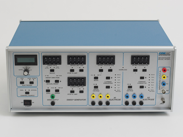
A complete CBP bipotentiostat system is a combination of the bipotentiostat itself, an interface board and cable (manufactured by National Instruments), and a Windows-based desktop computer (usually provided by the customer). With any system made up of components from a variety of manufacturers, it is important to assure that all of the components are working together in the best possible configuration. In the specific case of the CBP bipotentiostat, a common issue is making sure that the interconnections between the components are made in such a way that excess signal noise is not introduced into the system. This article describes best practices for electrical connections (to eliminate most signal noise at its source) and for signal filtering (for removing noise as the signals are sampled).
When working with the CBP bipotentiostat system, it is very important to make certain that all parts of the system are properly grounded. The computer system, the monitor, and the bipotentiostat should all be connected to the same grounded power source (i.e., do not connect the computer and the bipotentiostat to different power circuits).
The metal chassis of the bipotentiostat is connected to the earth ground via the third prong on the power cord. The front panel of the bipotentiostat has a convenient binding post (in the lower right corner) that can be used to make additional earth grounding connections as needed. Typically, any metal object located near the electrochemical cell (such as a rotating disk electrode, a clamp holding the cell, or a Faraday cage around the cell) should be connected to the earth ground.
The various cables which connect the bipotentiostat to the electrochemical cell should be of the shielded (coaxial) type whenever possible. These cell cables should be routed well away from any power cords, network cables, or video monitors, all of which are considerable sources of electrical noise.
The cable which connects to the reference electrode must be of the shielded coaxial type. The shield of this cable is driven by the bipotentiostat to the same potential as the reference electrode. Thus, the shield line on the reference electrode cable should never be connected to ground.
There is a signal filter board installed inside the CBP bipotentiostat which filters the signals which travel through the interface cable. Both the excitation signals and the response signals are filtered using this board. Note that this board may not be present in some early model CBP bipotentiostats, but it may be obtained from Pine and installed in an existing CBP system. (click here for installation instructions)
[call_to_action]The waveforms applied by the interface board to the bipotentiostat are called the excitation signals. There is one excitation signal for each of the two working electrodes (K1 and K2). These excitation signals are generated by the interface board (which is installed in a Windows-based personal computer), and the signals travel through the interface cable to a connector on the back panel of the bipotentiostat. After passing through the back panel, these signals may be filtered to remove any digital noise from the computer that may have traveled through the interface cable.
There are three filtering options available for each excitation signal. One option is to allow the signal to pass through without any filtering. The other two options are low-pass filters with either a 10 Hz or 1 KHz cutoff frequency. The excitation signal filters for each signal (K1 and K2) may be set independently; however, it is common practice to apply the same amount of filtering to both signals.
The boxes below list the jumper settings for the filtering options available for the K1 and K2 excitation signals. The factory default settings use the 1 kHz filters for both K1 and K2.
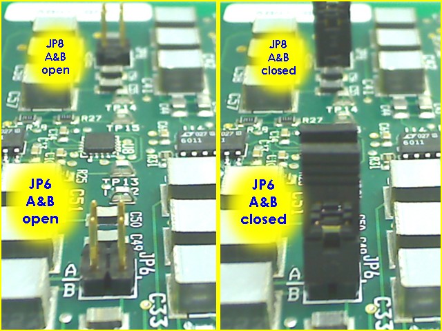
The two figures below show the proper configurations for the jumpers which control filtering of the excitation signals.

Example Settings for JP6 and JP8
Example Settings for JP7 and JP9
[/toggle] [toggle title = “Response Signal Filters”]The current and potential signals measured at both working electrodes are the four principle response signals which travel from the bipotentiostat back to the interface board through the interface cable. All four of these signals (E1, I1, E2, and I2) are filtered using low-pass filters. The cutoff frequency for all four low-pass filters is adjusted using jumpers JP1 and JP2 on the signal filter board. There are four different cutoff frequencies available (1, 10, 100, and 1 kHz). The frequency setting applies to all four signals (i.e., it is not possible to set the frequency individually for each response signal). The factory default settings use the 10 Hz filters for both K1 and K2.
The choice of cutoff frequency for the response signals may be placed under external software control (via the interface board) by setting the jumpers as shown in the figure below. This option is only available when using AfterMath (version 1.3 or higher) in conjunction with an M Series interface board (such as the PCI-6251). Contact Pine for further details.
The excitation signals generated by the interface board are (by default) referenced with respect to the analog output ground (AOGND) located on the interface board itself. It is possible to use a jumper on the filter board to cause the excitation signals to be referenced with respect to the local ground for the CBP bipotentiostat instead. This latter choice is not recommended at this time. Contact Pine for further details.
It is possible to connect the response signal ground reference from the CBP bipotentiostat (i.e., the DC Common) to any of three different ground references on the interface board. By default, no such connections are made. However, a jumper on the filter board can be used to connect the DC Common to one of three lines on the interface board (AOGND, AISENSE, or AIGND). Such connections are not recommended at this time. Contact Pine for further details.
An analog bipotentiostat circuit is based on a set of feedback loops built from operational amplifiers. In any such feedback system, there is a tradeoff between the response time of the system and the stability of the system. To increase the stability of the system, the response time of the system can be intentionally attenuated (i.e., slowed or damped). Conversely, adjusting the system to be more responsive may make the system prone to oscillations caused by constructive feedback and amplification of small noise signals.
When a potentiostat system is connected to a particular electrochemical cell, it is often necessary to tune the responsiveness of the instrument to match the cell geometry and type experiment being performed. In general, it is desirable to tune the potentiostat to the minimum amount of feedback attenuation required to guarantee stable operation. Finding the proper amount of attenuation is often a trial-and-error process.
On the back panel of the CBP bipotentiostat, there is a knob that can be used to adjust the amount of attenuation in the analog feedback circuits. This knob has four settings marked 0, 1, 2, and 3. The lowest setting (0) represents the least amount of attenuation (fastest instrument response time) while the highest setting (3) introduces a great deal of attenuation into the circuit (slow instrument response time).
Feedback Attenuation Knob (back panel)
When possible, the instrument should be operated with the feedback attenuation knob in position “0” or “1”. This allows the instrument to remain fairly responsive to sudden changes in signal levels without significant distortion.
In certain slow, steady-state experiments (such as rotating disk voltammetry and rotating ring-disk voltammetry), the attenuation knob can be adjusted to position “2” to provide even greater stability. Because such steady state experiments do not typically generate signals which change rapidly, the extra damping associated with position “2” is not a major concern.
Position “3” is not recommended except for those cases where signals remain constant over very long periods of time (i.e., very long-term electrolysis experiments).
Related Hardware Links: Filter Board Installation, CBP Bipotentiostat, Interface Boards
Related Software Links: AfterMath, PineChem, NIDAQ Device Driver

Request a Quote for this Cart
Below is the billing data we have on file. These details will be used on your quotation, so please update them here if you require any changes. Changing any details here updates them for your account.


